How Solder Mask Protects Modern Computer Circuit Boards
Printed circuit boards contain dense networks of copper traces, solder joints, pads, vias, and electronic components. Without a protective surface layer, these conductive areas would be more vulnerable to accidental contact, contamination, oxidation, and unwanted solder connections during manufacturing or repair.
Solder mask is the thin protective coating applied over most of the copper on a circuit board. It leaves selected pads exposed where components must be soldered while covering the surrounding conductors. This controlled exposure helps manufacturers assemble complex electronics accurately and gives finished boards greater protection during everyday operation.
What Solder Mask Is
Solder mask is an electrically insulating polymer layer bonded to the surface of a printed circuit board. It is normally applied after the copper circuitry has been formed but before components are installed.
The material covers copper traces and other areas that should remain insulated while openings are created around solder pads, test points, connectors, and selected exposed conductors. These openings allow solder to reach only the locations intended by the board design.
Solder mask does not create the circuit. It protects the copper circuitry already built into the board.
Why Most Circuit Boards Appear Green
Green is the color most commonly associated with solder mask, especially on motherboards, graphics cards, power supplies, and other computer hardware. Its widespread use developed because green provides good visual contrast with copper, solder, white silkscreen markings, and dark electronic components.
The contrast helps automated inspection systems and technicians identify defects, alignment problems, contamination, and damaged traces. Green materials are also widely available and well established in high-volume circuit board manufacturing.
Solder Mask Can Be Produced in Many Colors
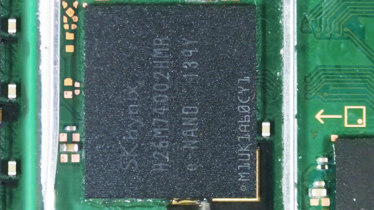
Although green remains common, solder mask is also manufactured in black, blue, red, white, yellow, purple, and other colors. Gaming motherboards, graphics cards, custom controllers, and specialty electronics often use alternative colors for appearance or product identification.
The color alone does not determine the quality or electrical performance of the board. Material formulation, application accuracy, curing, thickness, adhesion, and resistance to heat and chemicals are more important than appearance.
| Solder Mask Color | Common Reason for Use |
|---|---|
| Green | High contrast, widespread availability, and established manufacturing processes |
| Black | Premium appearance and reduced visibility of the underlying circuitry |
| Blue | Product differentiation and visual identification |
| Red | Distinctive appearance on gaming or specialty hardware |
| White | Reflective surfaces and selected lighting applications |
The Copper Beneath the Mask Carries Electrical Signals
The visible surface of a circuit board can make the solder mask appear to be the board itself, but the functional electrical pathways are formed by copper underneath it. These copper traces distribute power and carry signals between processors, memory, storage controllers, ports, sensors, and other components.
Because modern boards may contain extremely narrow traces positioned close together, protecting those conductors is essential. Even a small piece of conductive contamination can create an unintended connection between nearby circuits.
Preventing Unwanted Solder Bridges
During assembly, molten solder must remain around the correct component pads. If exposed copper existed between every pad, solder could spread across adjacent conductors and create bridges.
A solder bridge is an unwanted electrical connection formed when solder joins two areas that should remain separate. Depending on the circuit, this can cause startup failure, short circuits, incorrect signals, unstable operation, or permanent component damage.
- Solder mask separates closely spaced pads.
- It helps control how far molten solder can spread.
- It reduces accidental connections during automated assembly.
- It makes fine-pitch component installation more practical.
- It helps technicians identify where solder should and should not be present.
Fine-Pitch Components Depend on Accurate Mask Openings
Modern processors, memory chips, controllers, and power-management devices may have dozens or hundreds of electrical connections placed very close together. The openings in the solder mask must align accurately with the copper pads beneath them.
If an opening is too large, more copper may be exposed than necessary, increasing the possibility of solder bridging. If it is too small or misaligned, part of the pad may be covered, making a reliable solder joint more difficult to create.
Solder Mask Helps Protect Against Oxidation
Bare copper reacts with oxygen and moisture in the surrounding environment. Over time, this reaction creates oxidation that changes the surface condition of the metal.
By covering most of the copper circuitry, solder mask reduces direct exposure to air, humidity, fingerprints, and common contaminants. Exposed pads still require their own protective surface finish, but the masked traces receive an additional barrier against environmental contact.
The Mask Provides Limited Mechanical Protection
Solder mask is not a structural reinforcement layer, but it offers some protection against light abrasion and handling. It helps prevent tools, loose hardware, cables, and debris from directly touching delicate copper traces.
This protection has limits. A screwdriver, sharp probe, metal bracket, or excessive scraping force can cut through the coating and damage the copper beneath it.
A circuit board surface can look only lightly scratched while the copper trace underneath has already been weakened or severed.
Solder Mask Is Not Conformal Coating
Solder mask and conformal coating are sometimes confused because both cover portions of a circuit board. Their purposes and application stages are different.
Solder mask is part of the board manufacturing process and primarily covers the copper circuitry before component assembly. Conformal coating is usually applied after components have been installed and may cover solder joints, component leads, and other assembled areas to provide additional environmental protection.
| Protective Material | Primary Role |
|---|---|
| Solder mask | Covers copper traces and controls exposed soldering areas |
| Conformal coating | Protects an assembled circuit board from moisture and contamination |
| Silkscreen | Adds printed labels, symbols, outlines, and component references |
| Surface finish | Protects exposed copper pads and supports solderability |
Silkscreen Markings Sit Above the Solder Mask
The letters, numbers, outlines, polarity symbols, and component labels printed on a circuit board are normally part of the silkscreen layer. This information helps manufacturers, repair technicians, and inspectors identify component locations and orientation.
The silkscreen is usually printed over the solder mask rather than directly onto the copper. Damage that removes the printed marking does not always mean the electrical circuit beneath it has been harmed, although deeper scratches should still be inspected carefully.
Openings in the Mask Are Deliberate
Not every exposed metal area on a circuit board indicates damage. Component pads, connector contacts, grounding points, test points, mounting areas, and thermal surfaces may be intentionally left uncovered.
These openings are created according to the board design. Their size and location are controlled so the exposed copper can be soldered, tested, contacted, or connected to another conductive surface.
Test Points Must Remain Accessible
Manufacturers and repair technicians use test points to measure voltage, resistance, signal activity, and circuit continuity. These locations are often small exposed pads distributed throughout the board.
Because a test probe must make electrical contact, the solder mask is removed from the selected area. The presence of a small uncovered pad is therefore normal when it matches the intended board layout.
Vias May Be Covered or Exposed
Vias are small plated holes that carry electrical connections between different copper layers inside a printed circuit board. Depending on the design, they may remain open, be covered by solder mask, or be filled and sealed.
Covering a via with solder mask is often called tenting. Tented vias reduce exposed conductive areas and can help prevent solder from entering or flowing through the hole during assembly.
The Mask Must Withstand Soldering Temperatures
During manufacturing and repair, circuit boards are exposed to temperatures high enough to melt solder. The solder mask must remain bonded to the board without blistering, peeling, or losing its insulating properties under properly controlled conditions.
Excessive heat, repeated rework, poor-quality materials, or incorrect soldering techniques can weaken the coating. Once damaged, the affected area may expose copper or allow contamination beneath the lifted material.
Heat Damage Can Change the Appearance of the Surface
A circuit board exposed to excessive soldering heat may develop darkened areas, bubbling, cracking, or separation around pads and traces. Some discoloration may be cosmetic, while more severe changes can indicate damage to the mask, copper adhesion, or underlying board material.
Inspection should consider whether the pad remains firmly attached, whether nearby traces are intact, and whether the damaged coating still provides adequate separation between conductive areas.
Flux Residue Can Collect Around Damaged Mask
Flux is used during soldering to improve wetting and remove surface oxidation. Depending on the flux type and repair process, residue may remain around component pads after work is completed.
A smooth, intact solder mask is generally easier to clean than a surface with scratches, lifted edges, or exposed fiberglass. Damaged areas can trap residue and contamination, making careful cleaning and inspection more important.
Scratches Can Expose Conductive Copper
Surface scratches are common on boards that have been handled, removed from a chassis, or repaired previously. A light mark that affects only the upper surface may not create an electrical problem.
Deeper scratches can remove the solder mask and expose copper traces. Once exposed, the trace becomes more vulnerable to corrosion, accidental contact, and further mechanical damage. If the copper itself is cut, the circuit may become intermittent or completely open.
Repair Work May Require Removing a Small Amount of Mask
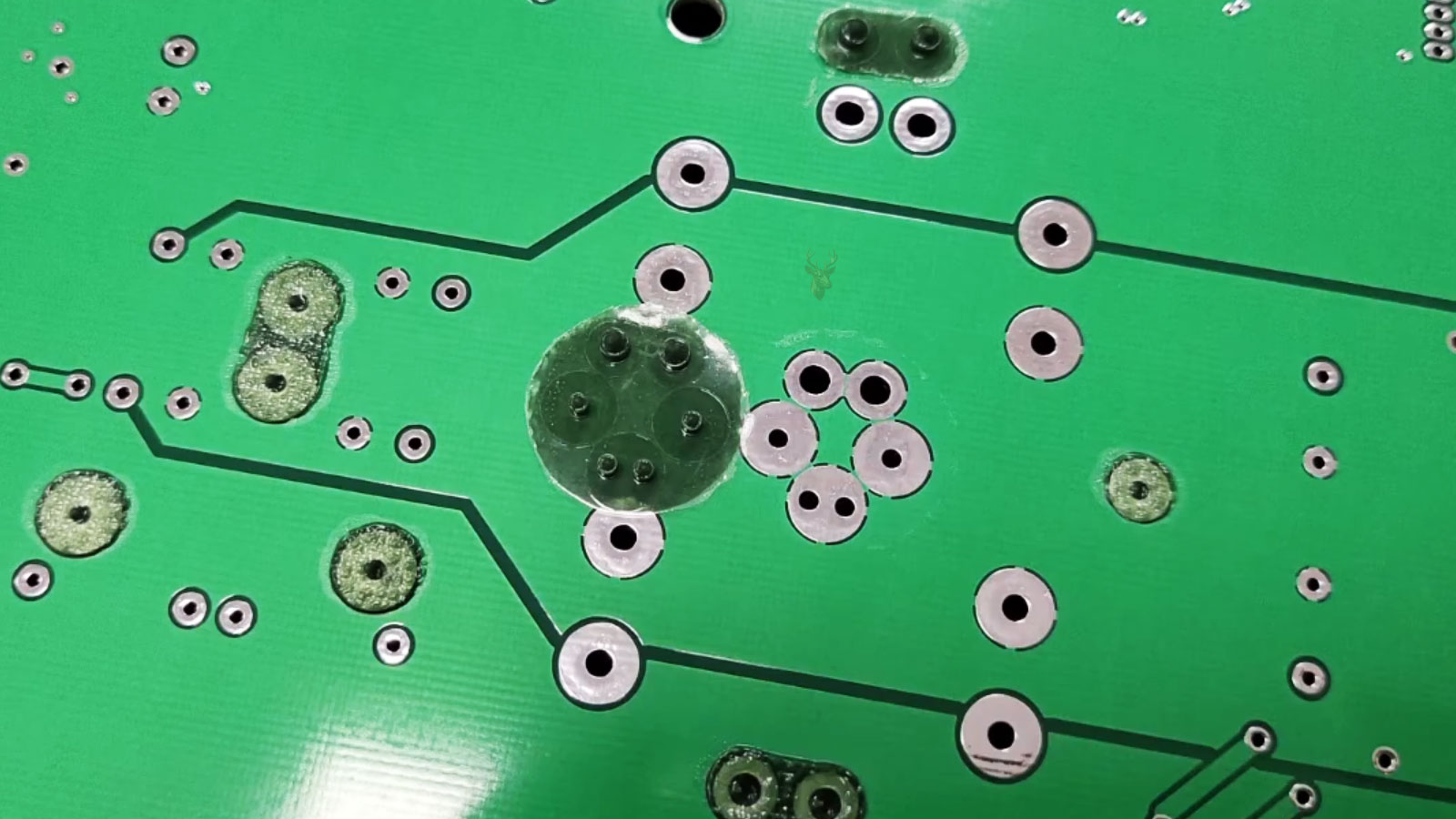
During component-level repair, a technician may intentionally scrape away a controlled section of solder mask to access a damaged trace or create a new solder connection. This is sometimes necessary when a pad has lifted, a conductor has broken, or a jumper wire must be attached.
The exposed area should be kept as small as practical. Removing more coating than necessary increases the risk of damaging adjacent traces and reduces the protection provided by the original board surface.
Damaged Areas Often Need to Be Resealed
After a trace repair or jumper installation has been completed and tested, exposed conductive areas may require a suitable protective coating. Resealing helps reduce the chance of corrosion, movement, contamination, and accidental contact with nearby metal.
The repair material must be appropriate for electronic circuit boards and should not interfere with connectors, test points, grounding surfaces, or components that need to dissipate heat.
Solder Mask Supports Dense Computer Hardware Designs
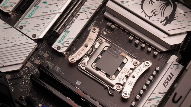
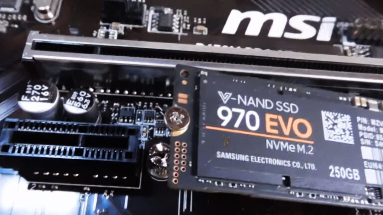
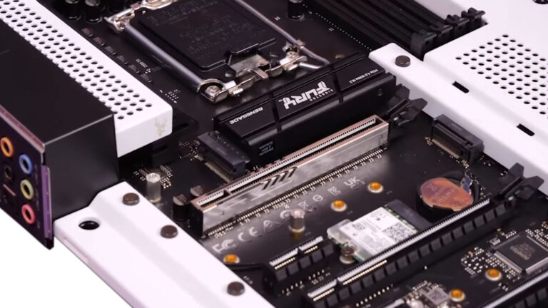
Motherboards, graphics cards, storage devices, laptop logic boards, and power supplies place large numbers of electrical connections into limited space. Solder mask allows these circuits to be positioned closely while maintaining separation between conductive areas.
Its protective role is easy to overlook, but modern computer hardware would be more difficult to manufacture, inspect, solder, and repair without it. The condition of this thin surface layer can also reveal important clues about overheating, previous repair attempts, contamination, and physical damage.
Solder Mask Damage Can Reveal Previous Board Stress
Changes in solder mask condition can provide useful clues during circuit board inspection. Peeling, blistering, discoloration, cracking, or scraped areas may indicate overheating, mechanical damage, liquid exposure, manufacturing defects, or previous repair work.
The visible coating does not always reveal the full extent of the problem. Damage may extend into the copper trace, plated hole, pad, or fiberglass board material beneath the surface.
Blistering Can Develop After Excessive Heat
Blisters form when the solder mask lifts away from the board surface. This separation may occur after excessive soldering temperatures, prolonged overheating, trapped moisture, chemical exposure, or poor adhesion during manufacturing.
A blistered area should be inspected carefully because the lifted coating can trap residue or allow contamination to reach the copper underneath. If the copper has also separated from the board, the electrical connection may be weakened.
Discoloration Does Not Always Mean the Circuit Has Failed
Solder mask can darken after repeated exposure to heat, flux, cleaning agents, or normal aging. A color change by itself does not confirm that the copper trace or component beneath it has failed.
Inspection should consider whether the surface is still firmly attached, whether the board material has charred, whether nearby solder joints remain intact, and whether electrical measurements show a problem in the affected circuit.
Visual changes provide evidence, but electrical testing is still required to determine whether the circuit remains functional.
Burned Board Material Requires Careful Evaluation
Severe overheating can damage more than the solder mask. The underlying fiberglass and resin may become dark, brittle, cracked, or carbonized. Carbonized board material can become partially conductive and create leakage paths between circuits.
Cleaning the visible surface may not correct this condition. Damaged material may need to be removed, isolated, or rebuilt before the board can operate safely and reliably.
Liquid Damage Can Travel Beneath the Surface
Solder mask helps limit direct exposure of copper traces, but it does not make a circuit board waterproof. Liquids can enter through component pads, connectors, vias, damaged coating, board edges, and areas where the mask does not fully seal around metal surfaces.
Once moisture reaches exposed copper, corrosion can develop beneath components or along the edge of damaged mask. The visible stain may appear small even when the affected conductive area is larger.
- Corrosion may spread from exposed pads into nearby traces.
- Residue can remain under connectors and integrated circuits.
- Lifted mask edges can trap moisture and contamination.
- Damaged vias can interrupt connections between board layers.
- Electrical leakage may continue after the surface appears dry.
Corrosion Often Begins at Exposed Metal
Component leads, solder joints, test points, connector contacts, and damaged traces provide locations where moisture and contaminants can reach conductive metal. Corrosion may gradually increase resistance, weaken solder joints, or completely remove thin copper pathways.
Areas covered by intact solder mask are generally better protected, but corrosion can still move underneath the coating if it enters through a damaged edge or opening.
Lifted Pads Affect Both Soldering and Electrical Continuity
A solder pad is the exposed copper area where a component lead or terminal is attached. Excessive heat, pulling force, repeated rework, or mechanical stress can separate the pad from the board surface.
When a pad lifts, the surrounding solder mask may crack or peel with it. The component may still appear soldered, but the pad can lose its connection to the trace or plated hole that carries the signal into the rest of the circuit.
| Visible Condition | Possible Concern |
|---|---|
| Scraped solder mask | Exposed or damaged copper trace |
| Lifted pad | Broken connection between the component and circuit |
| Blistered coating | Heat damage, poor adhesion, or trapped contamination |
| Darkened board area | Thermal stress or carbonized board material |
| Green or white residue | Corrosion involving copper, solder, or component leads |
Trace Damage Can Produce Intermittent Symptoms
A copper trace does not always fail completely when scratched or weakened. A narrow section may continue conducting electricity while developing higher resistance or losing contact only when the board flexes, heats, or cools.
This can produce problems that appear and disappear, including failed startup, missing ports, unstable charging, intermittent display output, memory errors, or components that work only when pressure is applied near the damaged area.
Multilayer Boards Make Damage More Difficult to Follow
Modern motherboards and graphics cards contain several internal copper layers. A visible surface trace may connect through a via to pathways hidden inside the board.
If a via is damaged, corrosion may interrupt an internal connection that cannot be inspected directly from the surface. Continuity testing, schematic information, board-view data, and comparison with a known working circuit may be needed to locate the break.
Solder Mask Can Hide Very Fine Traces
Some copper pathways are too narrow to distinguish clearly beneath an opaque solder mask. Technicians may use magnification, strong directional lighting, continuity measurements, or circuit documentation to determine where a trace travels.
Removing mask without first understanding the route of the circuit can damage adjacent conductors. Controlled access is especially important around processors, memory, charging controllers, and fine-pitch connectors.
Board Flexing Can Crack the Protective Surface
Circuit boards can flex during installation, removal, connector insertion, screw tightening, or physical impact. Repeated flexing may create hairline cracks in solder joints, copper traces, vias, and the solder mask covering them.
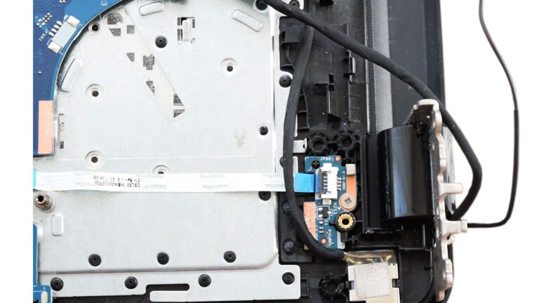
Laptop logic boards are particularly vulnerable when damaged hinges, swollen batteries, bent cases, or incorrect screw placement place continuous pressure on the board.
A cracked surface coating may be a visible sign of mechanical stress affecting less visible electrical connections underneath.
Incorrect Screws Can Cut Into a Circuit Board
Computer manufacturers often use screws of different lengths within the same device. Installing a longer screw in the wrong location can press against or puncture a circuit board.
The damage may remove solder mask, cut copper traces, crush internal layers, or create a short circuit against the metal screw. Careful screw organization during disassembly helps prevent this type of repair-related damage.
Sharp Tools Can Cause Hidden Electrical Problems
Metal tools used near a circuit board can slip and scrape across the surface. A screwdriver, tweezers, probe, or pry tool may remove only a narrow line of solder mask while severing one or more fine traces beneath it.
Because the damaged area may be extremely small, the resulting failure can be mistaken for a defective component or firmware problem unless the board is inspected under magnification.
Metal Debris Can Bridge Exposed Conductors
Loose screws, clipped component leads, solder fragments, wire strands, and metallic dust can create unintended electrical connections when they contact exposed pads or damaged traces.
Intact solder mask reduces the amount of exposed conductive surface, but it cannot prevent every short circuit. Careful cleaning and inspection remain necessary after soldering or mechanical repair work.
Repair Areas Must Be Clean Before Resealing
Applying protective coating over flux residue, corrosion, moisture, or loose material can trap contamination against the circuit. The damaged area should be cleaned, dried, inspected, and electrically tested before new mask or another suitable coating is applied.
Any exposed copper should also be checked for continuity, secure adhesion, and proper separation from neighboring conductors.
Ultraviolet-Curable Mask Is Common in Board Repair
Some repair technicians use ultraviolet-curable solder mask to protect exposed traces and secure small jumper wires. The liquid material is positioned over the repair and hardened with ultraviolet light.
Correct application requires controlling the thickness and keeping the material away from connector contacts, component pads, test points, and other surfaces that must remain electrically accessible.
Protective Coating Should Not Replace a Weak Connection
Solder mask can cover and stabilize a completed repair, but it cannot restore electrical continuity by itself. Broken traces, loose pads, damaged vias, and incomplete solder joints must be repaired before the area is sealed.
Coating an unreliable connection may make later inspection more difficult without improving the operation of the circuit.
Professional Inspection Combines Visual and Electrical Testing
Board-level diagnosis rarely depends on appearance alone. Technicians may inspect the solder mask under magnification, test trace continuity, compare resistance readings, verify voltages, examine thermal behavior, and evaluate the surrounding components.
Combining these methods helps determine whether the visible damage is cosmetic, whether the copper beneath it has been affected, and whether the repaired circuit can remain reliable during normal operation.
Solder Mask Quality Begins During Board Manufacturing
The protective value of solder mask depends heavily on how accurately it is applied and cured. Uneven thickness, trapped contamination, poor adhesion, incorrect exposure, or incomplete curing can leave parts of the copper circuitry more vulnerable than intended.
High-quality manufacturing controls the location of every opening, the consistency of the coating, and the bond between the mask and the circuit board surface. These details become especially important on densely populated boards with narrow traces and closely spaced component pads.
Liquid Photoimageable Solder Mask Is Widely Used
Many modern printed circuit boards use liquid photoimageable solder mask. The material is spread across the board, selectively exposed to ultraviolet light through a patterned image, developed to remove uncured areas, and then fully hardened.
This process allows manufacturers to create precise openings around pads, vias, test points, and connectors. Accurate imaging is essential because even a small alignment error can partially cover a solder pad or expose more copper than the design allows.
Mask Alignment Affects Solder Joint Quality
The boundary between the solder mask and each exposed copper pad must be positioned correctly. If the mask extends too far onto the pad, it can reduce the usable soldering area and interfere with proper wetting.
If the opening extends too far beyond the pad, nearby copper may become exposed. On fine-pitch components, that extra exposure can increase the chance of solder bridging or contamination between adjacent electrical connections.
- Correct alignment preserves the intended pad dimensions.
- Consistent openings support uniform solder joints.
- Controlled spacing reduces the chance of solder bridges.
- Accurate registration improves automated optical inspection.
- Proper coverage protects narrow traces near component pads.
Solder Mask Defined Pads and Non-Solder Mask Defined Pads
Circuit board designers can control a soldering surface through either the copper pad dimensions or the opening in the solder mask. These approaches are commonly described as solder mask defined and non-solder mask defined pads.
With a solder mask defined pad, the opening in the mask is smaller than the copper pad underneath. The edge of the solderable area is therefore determined by the mask. With a non-solder mask defined pad, the mask opening is larger than the copper pad, leaving the full copper pad exposed.
| Pad Design | How the Soldering Area Is Controlled |
|---|---|
| Solder mask defined | The mask opening determines the exposed soldering surface |
| Non-solder mask defined | The copper pad dimensions determine the soldering surface |
The selected design depends on component type, manufacturing tolerances, pad strength, solder behavior, and the spacing available between connections.
Very Small Mask Barriers Can Be Difficult to Manufacture
The narrow strip of solder mask between two neighboring pads is sometimes called a solder mask dam or web. This barrier helps prevent molten solder from joining adjacent connections.
As pad spacing becomes smaller, the mask barrier may become too narrow to apply reliably. Manufacturers may need to adjust the opening design, use tighter production tolerances, or remove the barrier entirely in selected areas.
Component Packages Place Different Demands on the Mask
A large through-hole connector does not require the same solder mask precision as a fine-pitch controller or ball grid array package. Each component style creates different requirements for pad spacing, thermal behavior, solder flow, and inspection.
Dense processors and memory devices may contain connections hidden beneath the component body. In these areas, accurate mask openings help control solder placement even though the finished joints cannot be viewed directly from above.
Ball Grid Array Components Require Precise Board Preparation
Ball grid array components connect to the circuit board through an array of solder balls located underneath the package. The pad design and solder mask openings must support consistent ball alignment and solder flow during reflow.
Misaligned mask, contaminated pads, warped boards, incorrect solder volume, or uneven heating can contribute to open connections, bridged joints, or weak solder bonds beneath the component.
When solder joints are hidden beneath a component, manufacturing accuracy becomes even more important because direct visual inspection is limited.
Thermal Pads May Contain Several Masked or Exposed Vias
Power-management chips, processors, and other heat-producing components may use a large center pad to transfer heat into the circuit board. Thermal vias can carry that heat into internal copper layers or to the opposite side of the board.
The treatment of these vias affects solder movement. Open vias may draw solder away from the pad, while filled, capped, or carefully masked vias can help preserve the intended solder volume beneath the component.
Solder Mask Thickness Must Remain Controlled
A coating that is too thin may provide inadequate coverage over trace edges and uneven copper surfaces. A coating that is too thick can interfere with component seating, connector fit, or the flatness required around certain packages.
Manufacturing specifications therefore control both the overall thickness and the minimum coverage over critical areas. The correct value depends on the board construction, material system, copper thickness, and intended use.
Curing Gives the Mask Its Final Properties
After imaging and development, the solder mask must be fully cured. Proper curing strengthens adhesion and helps the material resist heat, chemicals, moisture, handling, and repeated thermal changes.
Incomplete curing can leave the surface softer, more chemically sensitive, or less firmly bonded to the board. Overheating during curing can also affect appearance or material performance, so temperature and exposure must remain controlled.
Surface Cleanliness Affects Adhesion
Before solder mask is applied, the copper and board surface must be properly prepared. Oils, oxidation, dust, moisture, or chemical residue can prevent the coating from bonding evenly.
Poor adhesion may not become obvious immediately. The mask can later lift during soldering, cleaning, thermal cycling, or mechanical handling, exposing copper that was originally intended to remain protected.
Board Edges and Cutouts Need Careful Inspection
Circuit board edges, mounting holes, slots, and internal cutouts can place the solder mask close to routed or drilled surfaces. Mechanical fabrication may chip the coating if the material is poorly bonded or if the cutting process places excessive stress on the board.
Exposed copper near an edge is especially important to evaluate because it may contact a metal chassis, mounting bracket, shield, or screw. Some exposed areas are intentional grounding points, while others may indicate damage.
Mounting Holes May Be Grounded or Electrically Isolated
Some circuit board mounting holes include exposed copper connected to the ground plane. These areas may be designed to contact a conductive standoff or screw and establish chassis grounding.
Other mounting holes are intended to remain isolated. Applying solder, coating, washers, or replacement hardware without understanding the design can change the electrical relationship between the board and the chassis.
Connector Contacts Must Remain Free of Protective Coating
Edge connectors, memory contacts, expansion card fingers, keyboard connectors, and other electrical contact surfaces must remain accessible. Solder mask, repair coating, adhesive, or cleaning residue on these areas can prevent a reliable connection.
When resealing a nearby repair, technicians must control the material carefully so it does not flow onto contact surfaces or into connector openings.
Gold Fingers Use a Different Surface Protection Method
The exposed contacts along graphics cards, memory modules, and expansion boards are often called gold fingers. These conductive surfaces repeatedly slide into a connector and therefore cannot be covered by solder mask.
Instead, they use a durable metallic finish designed to resist oxidation and support repeated insertion. The solder mask normally stops at a controlled distance from the contact area.
Cleaning Chemicals Must Be Compatible With the Board
Circuit boards may be cleaned after manufacturing or repair to remove flux, oils, dust, and contamination. The selected cleaner must be appropriate for the solder mask, component materials, adhesives, labels, and plastics present on the assembly.
Harsh chemicals or prolonged soaking can soften, stain, or weaken certain coatings. Cleaning should also avoid leaving conductive or sticky residue behind.
- Use electronics-compatible cleaning materials.
- Avoid flooding connectors and sensitive mechanical parts.
- Allow the board to dry completely before applying power.
- Inspect damaged mask edges for trapped residue.
- Confirm that labels, thermal pads, and adhesives remain secure.
Replacement Mask Must Be Selected for the Repair Environment
Not every colored coating is suitable for repairing a circuit board. Nail polish, general-purpose paint, household adhesive, and unrelated sealants may contain solvents, remain conductive under certain conditions, soften with heat, or release contamination.
A proper repair material should be intended for electronic use and compatible with the operating temperature, voltage, board-cleaning process, and physical space around the repaired circuit.
Color Matching Is Usually Secondary to Electrical Protection
A repaired section may not perfectly match the original board color. Although appearance can help identify the repair area, electrical insulation, adhesion, heat resistance, and complete coverage are more important than achieving an exact cosmetic match.
The repaired area should remain easy to inspect and should not conceal an incomplete solder joint, unstable jumper, or unresolved corrosion problem.
Jumper Wires Need Mechanical Support
A jumper wire may restore continuity when an original trace or pad can no longer be used. The electrical connection must be soldered securely, but the wire also needs protection from movement.
A suitable mask or board-repair coating can hold the wire against the surface and reduce stress on the soldered endpoints. The coating should not pull the wire out of position while curing or cover areas that may require later testing.
High-Voltage Areas Require Adequate Separation
Power supplies, inverter circuits, charging systems, and other high-voltage sections require controlled spacing between conductors. Solder mask provides insulation, but it does not eliminate the need for correct clearance and creepage distances in the board design.
Burned residue, conductive contamination, exposed copper, poor repairs, or carbonized board material can reduce effective separation and create leakage or arcing risks.
Protective coating supports electrical isolation, but safe spacing must already exist within the circuit design.
Repeated Heating and Cooling Can Weaken Damaged Areas
Computer hardware repeatedly heats during use and cools after shutdown. Copper, solder, fiberglass, components, and solder mask expand and contract at different rates.
An intact board is designed to tolerate normal thermal cycling, but cracked coating, lifted pads, weakened traces, or poorly secured repairs may deteriorate over time. A connection that passes an initial test can still fail later if the mechanical repair is incomplete.
Burn-In Testing Can Help Confirm Repair Stability
After a board-level repair, the computer may need to operate under controlled load while temperatures, voltages, charging behavior, ports, and system stability are monitored. This testing can expose connections that fail only after warming or under increased electrical demand.
Visual inspection should be repeated after testing to confirm that the replacement coating has not lifted, cracked, softened, or shifted around the repaired area.
A Good Repair Preserves Future Serviceability
Protective material should secure the completed repair without making later diagnosis unnecessarily difficult. Test points, connector contacts, component markings, and nearby solder joints should remain accessible whenever possible.
Documenting the location of trace repairs and jumper wires can also help future technicians understand why the board differs from its original layout.
Not Every Damaged Board Is Economical to Repair
A small scratched trace or lifted pad may be repairable, but widespread corrosion, internal-layer damage, carbonized material, multiple missing pads, or severe board delamination can make reliable restoration difficult.
The decision should consider the value of the equipment, availability of replacement boards, importance of stored data, safety of the affected circuit, and the likelihood that hidden damage will cause additional failures.
| Board Condition | Typical Repair Consideration |
|---|---|
| Minor mask scratch with intact copper | Clean, inspect, test, and reseal if necessary |
| Single broken surface trace | Restore continuity and protect the repair |
| Lifted pad with accessible connection | Rebuild or bypass the connection and secure it mechanically |
| Corrosion beneath several components | Remove contamination and evaluate the full affected circuit |
| Carbonized or delaminated board material | Assess safety, internal damage, and whether replacement is more practical |
Solder Mask Condition Is One Part of a Complete Diagnosis
The color and condition of the board surface can reveal overheating, corrosion, tool damage, previous soldering, lifted pads, and manufacturing irregularities. These findings help direct testing but should not be treated as proof of a specific failure without electrical confirmation.
A complete diagnosis considers the solder mask together with component condition, solder joint quality, voltage measurements, resistance readings, thermal behavior, firmware activity, and the symptoms reported during operation.
A Thin Layer With an Important Role
Solder mask may appear to be little more than the colored surface of a circuit board, but it performs several essential functions. It insulates closely spaced conductors, controls where solder can flow, limits copper exposure, supports accurate assembly, and provides a degree of protection from contamination and handling.
Its condition also matters during repair. Scraping, overheating, corrosion, lifted pads, and improper resealing can turn a small surface defect into an intermittent or permanent circuit failure. Careful inspection and controlled repair methods help preserve both electrical continuity and physical protection.
As computer hardware continues to place more circuitry into smaller spaces, the accuracy and reliability of solder mask remain increasingly important. This thin protective layer helps modern motherboards, graphics cards, storage devices, power circuits, and laptop logic boards operate safely within extremely dense electronic designs.